Home / Products / Components / Gate-Driver
| Place of Origin: | Zhejiang |
| Brand Name: | Inventchip Technology |
| Model Number: | IVCR1402DPQR |
| Certification: | AEC-Q100 qualified |
1. Features
• Driver current capacity: 4A sink and source peak drive current
• Wide VCC range up to 35V
• Integrated 3.5V negative bias
• Designed for low side and suitable for bootstrap high-side power
• UVLO for positive and negative gate drive voltage
• Desaturation detection for short circuit protection with internal blanking time
• Fault output when UVLO or DESAT detected
• 5V 10mA reference for external circuit, e.g. digital isolator
• TTL and CMOS compatible input
• SOIC-8 with exposed pad for high frequency and power applications
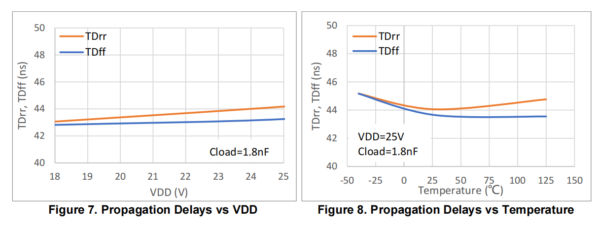
• Low propagation delay 45ns typical with build-in de-glitch filter
• AEC-Q100 qualified
2. Applications
• EV On Board Chargers
• EV/HEV inverters and charging stations
• AC/DC and DC/DC converters
• Motor Drive
3. Description
The IVCR1402Q is an AEC-Q100 qualified, 4A single-channel,high-speed smart driver,capable of efficiently and safely driving SiC MOSFETs and IGBTs. Strong drive with a negative bias improves noise immunity against Miller effect at high dv/dt operation.Desaturation detection provides robust short circuit protection and reduces the risk of power device and system component damage. A fixed 200ns blanking time is inserted to prevent overcurrent protection from being prematurely trigged by switching edge current spike and noise. Fixed positive gate drive voltage UVLO and fixed negative bias UVLO protection ensures healthy gate operation voltages. An active low fault signal alerts system when UVLO or over current happens. Low propagation delay and mismatch with an exposed thermal pad enables SiC MOSFETs to switch at hundreds of kHz. Integrated negative voltage generation and 5V reference output minimize external component count. It is the first industrial SiC MOSFET and IGBT driver which includes negative voltage generation, desaturation and UVLO in an 8-pin package. It is an ideal driver for a compact design.
Device Information
| PARTNUMBER | PACKAGE | PACKING | ||||||||||||||||||
| IVCR1402DPQR | SOIC-8 (EP) | Tape and Reel | ||||||||||||||||||

4. Pin Configuration and Functions
| PIN | NAME | I/O | DESCRIPTION | |||||||||||||||||||||||||||||||||||||||||
| 1 | IN | I | Logic input | |||||||||||||||||||||||||||||||||||||||||
| 2 | 5VREF | O | 5V/10mA output for external circuit | |||||||||||||||||||||||||||||||||||||||||
| 3 | /FAULT | O | Open collector fault output, pulled to low when over current orUVLO is detected. | |||||||||||||||||||||||||||||||||||||||||
| 4 | DESAT | I | Desaturation detection input | |||||||||||||||||||||||||||||||||||||||||
| 5 | VCC | P | Positive bias supply | |||||||||||||||||||||||||||||||||||||||||
| 6 | OUT | O | Gate driver output | |||||||||||||||||||||||||||||||||||||||||
| 7 | GND | G | Driver ground | |||||||||||||||||||||||||||||||||||||||||
| 8 | NEG | O | Negative voltage output | |||||||||||||||||||||||||||||||||||||||||
| Exposed pad | Bottom exposed pad is often tied to GND on layout. | |||||||||||||||||||||||||||||||||||||||||||
5. Specifications
5.1 Absolute Maximum Ratings
Over free-air temperature range (unless otherwise noted) (1)
| MIN MAX | UNIT | ||||||||||||||||||||||||||||||||||||||||||
| VCC Total supply voltage (reference to GND) | -0.3 35 | V | |||||||||||||||||||||||||||||||||||||||||
| VOUT Gate driver output voltage | -0.3 VCC+0.3 | V | |||||||||||||||||||||||||||||||||||||||||
| IOUTH Gate driver output source current (at max pulse width 10us and 0.2% duty cycle) | 6.6 | A | |||||||||||||||||||||||||||||||||||||||||
| IOUTL Gate driver output sink current (at max pulse width 10us and 0.2% duty cycle) | 6.6 | A | |||||||||||||||||||||||||||||||||||||||||
| VIN IN signal voltage | -5.0 20 | V | |||||||||||||||||||||||||||||||||||||||||
| I5VREF 5VREF output current | 25 | mA | |||||||||||||||||||||||||||||||||||||||||
| VDESAT Voltage at DESAT | -0.3 VCC+0.3 | V | |||||||||||||||||||||||||||||||||||||||||
| VNEG Voltage at NEG pin | OUT-5.0 VCC+0.3 | V | |||||||||||||||||||||||||||||||||||||||||
| TJ Junction temperature | -40 150 | °C | |||||||||||||||||||||||||||||||||||||||||
| TSTG Storage temperature | -65 150 | °C | |||||||||||||||||||||||||||||||||||||||||
(1) Operating beyond those listed under Absolute Maximum Ratings may cause permanent damage to the device.
Exposure to absolute maximum rated conditions for extended period may affect
device reliability.
5.2 ESD Rating
| Value | UNIT | |||||||||||||||||||||||||||||||||||||||||||
| V(ESD) Electrostatic discharge | Human body model (HBM), per AEC Q100-002 | +/-2000 | V | |||||||||||||||||||||||||||||||||||||||||
| Charged-device model (CDM), per AEC Q100-011 | +/-500 | |||||||||||||||||||||||||||||||||||||||||||
5.3 Recommended Operation Conditions
| MIN | MAX | UNIT | ||||||||||||||||||||||||||||||||||||||||||
| VCC Total supply voltage (reference to GND) | 15 | 25 | V | |||||||||||||||||||||||||||||||||||||||||
| VIN Gate input voltage | 0 | 15 | V | |||||||||||||||||||||||||||||||||||||||||
| VDESAT Voltage at DESAT | 0 | VCC | V | |||||||||||||||||||||||||||||||||||||||||
| TAMB Ambient temperature | -40 | 125 | °C | |||||||||||||||||||||||||||||||||||||||||
5.4 Thermal Information
| IVCR1402DPQR | UNIT | ||||||||||||||||||||||||||||||||||||||||||
| RθJA Junction-to-Ambient | 39 | °C/W | |||||||||||||||||||||||||||||||||||||||||
| RθJB Junction-to-PCB | 11 | °C/W | |||||||||||||||||||||||||||||||||||||||||
| RθJP Junction-to-exposed pad | 5.1 | °C/W | |||||||||||||||||||||||||||||||||||||||||
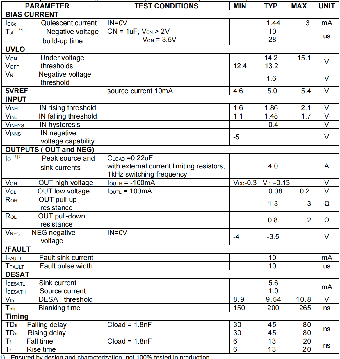
5.5 Electrical Specifications
Unless otherwise noted, VCC = 25 V, TA = –40°C to 125°C, 1-μF bypass capacitance from VCC to GND, f = 100 kHz.
Currents are positive into and negative out of the specified terminal. Typical condition specifications are at 25°C.
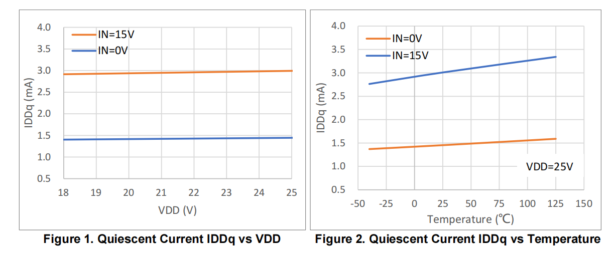
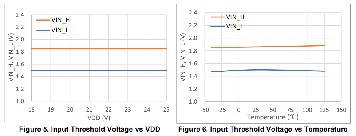
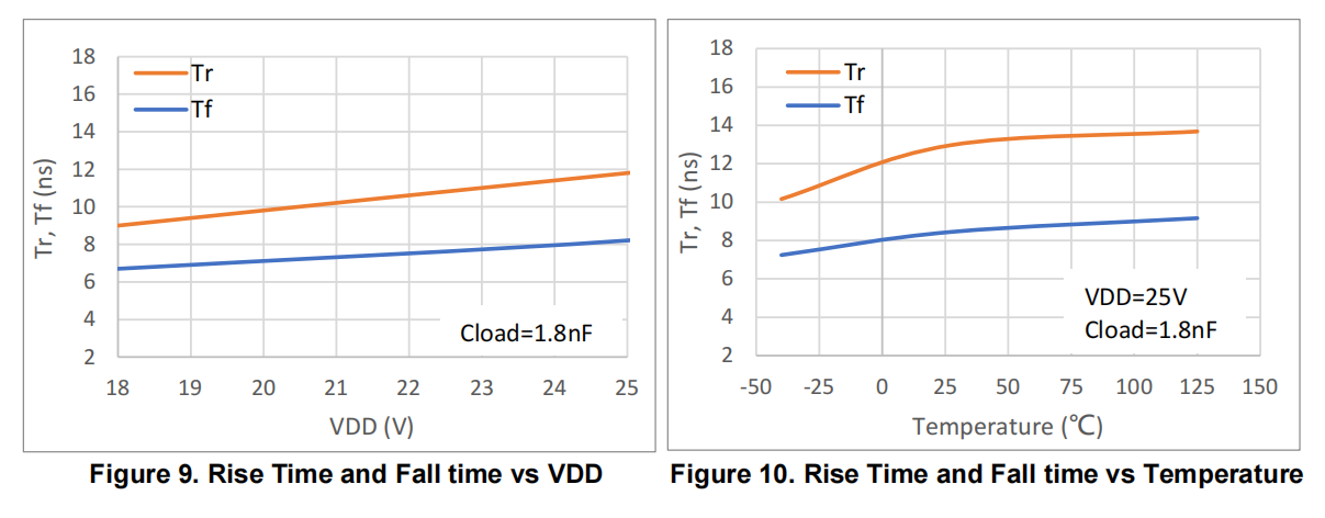
6 Typical Characteristics

7 Detail Description
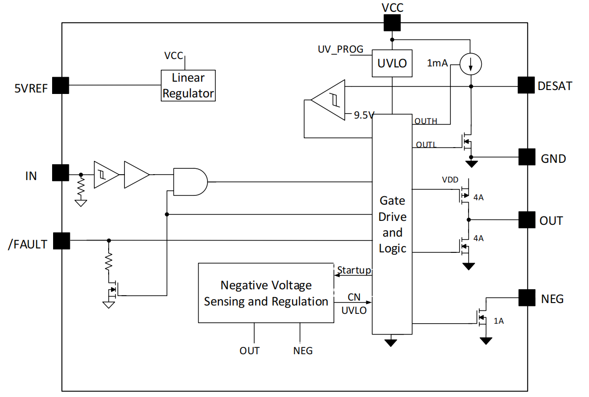
IVCR1402Q driver represents InventChip’s cutting-edge single channel low-side high-speed gate driver
technology development. It features built-in negative voltage generation, desaturation/short-circuit protection,
programmable UVLO. This driver offers the best-in-class characteristics and the most compact and reliable
SiC MOSFET gate driving control. It is the first industry driver equipped with all necessary SiC MOSFET gate
driving features in a SOIC-8 package.
Function Block Diagram
7.1 Input
IN is a non-inverting logic gate driver input. The pin has a weak pulldown. The input is a TTL and CMOS
compatible logic level with maximum 20V input tolerance.
7.2 Output
IVCR1402Q features a 4A totem-pole output stage. It delivers high peak source current when it is most
needed during the Miller plateau region of the power switch turn-on transition. Strong sink capability results in
a very low pull-down impedance in the driver output stage which improves immunity against parasitic Miller
turn-on effect, especially where low gate-charge Si MOSFETs or emerging wide bandgap SiC MOSFETs are
used.
7.3 Negative Voltage Generation
At startup, NEG output is pulled to GND and provides a high current path for a current source to charge the
external negative-voltage capacitor CN (1uF typical) through OUT pin. The capacitor can be charged to above
2.0V in less than 10us. Before the capacitor voltage, VCN, charged up, /FAULT stays low/active, disregarding
IN’s logic level. After the negative bias is ready, both NEG pin and /FAULT pin are released and OUT starts to
follow input signal IN. A built-in negative voltage regulator regulates the negative voltage to -3.5V for normal
operation, regardless of PWM frequency and duty cycle. The gate drive signal, NEG, then switches between
VCC-3.5V and -3.5V.
7.4 Under Voltage Protections
All internal and external biases of the driver are monitored to ensure a healthy operation condition. VCC is
monitored by a under voltage detection circuit. The driver output is shut down (pulled low) or stays low if the
voltage is below set limit. Note that VCC UVLO threshold is 3.5V higher than gate voltages.
The negative voltage is also monitored. Its UVLO has a fix 1.6V negative-going threshold. Negative voltage
capacitor defect could result in the capacitor voltage below the threshold. The UVLO protection will then pull
MOSFET’s gate to ground. The /FAULT is pulled low when UVLO is detected.
7.5 Desaturation Detection
When short circuit or over current happens, the power device’s (SiC MOSFET or IGBT) drain or collector
current can increase to such a high value that the devices get out of saturation state, and Vds/Vce of the
devices will rise to a substantially high value. DESAT pin with a blanking capacitor Cblk, normally clamped to
Id x Rds_on, now is able to charge up much higher by an internal 1mA constant current source. When the
voltage reaches typical 9.5V threshold, OUT and /FAULT are both pulled low. A 200ns blank time is inserted
at OUT rising edge to prevent DESAT protect circuit from being triggered prematurely due to Coss discharge.
To minimize the loss of internal constant current source, the current source is turned off when the main switch
is at off state. By selecting a different capacitance, turn-off delay time (external blanking time) can be
programmed. The blanking time can be calculated with,
Teblk = Cblk ∙Vth / IDESAT
For example, if Cblk is 47pF, Teblk = 47pF ∙9.5V / 1mA = 446ns.
Note Teblk includes internal Tblk 200ns blanking time already.
For current limit setting, the following equation can be used,
Ilimit = (Vth – R1* IDESAT – VF_D1)/ Rds_on
where R1 is a programming resistor, VF_D1 is high voltage diode forward voltage, Rds_on is SiC MOSFET turn
on resistance at estimated junction temperature, such as 175C.
A different power system usually requires a different turn-off time. An optimized turn-off time can maximize
the system short circuit capability while limiting Vds and bus voltage ringing.
7.6 Fault
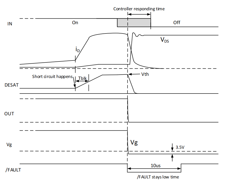
/FAULT is an open collector output with no internal pull-up resistance. When desaturation and under voltages
are detected, the /FAULT pin and OUT are both pulled low. The /FAULT signal will stay at low for 10us after
the fault condition is removed. /FAULT is an auto recovery signal. System controller will need to decide how
to respond the /FAULT signal. Following diagram shows the signal sequence.
7.7 NEG
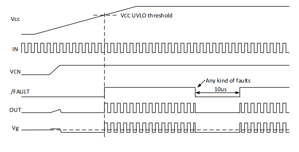
The external negative bias capacitor is quickly charged up when NEG goes low. It happens during power up
and restart period right before 10us /FAULT low period expires after any fault is detected. During power up
and restart period, the negative bias capacitor voltage VCN is measured. As soon as the voltage is beyond VN
UVLO threshold, NEG becomes high-impedance and OUT takes over gate drive control.
8 Applications and Implementation
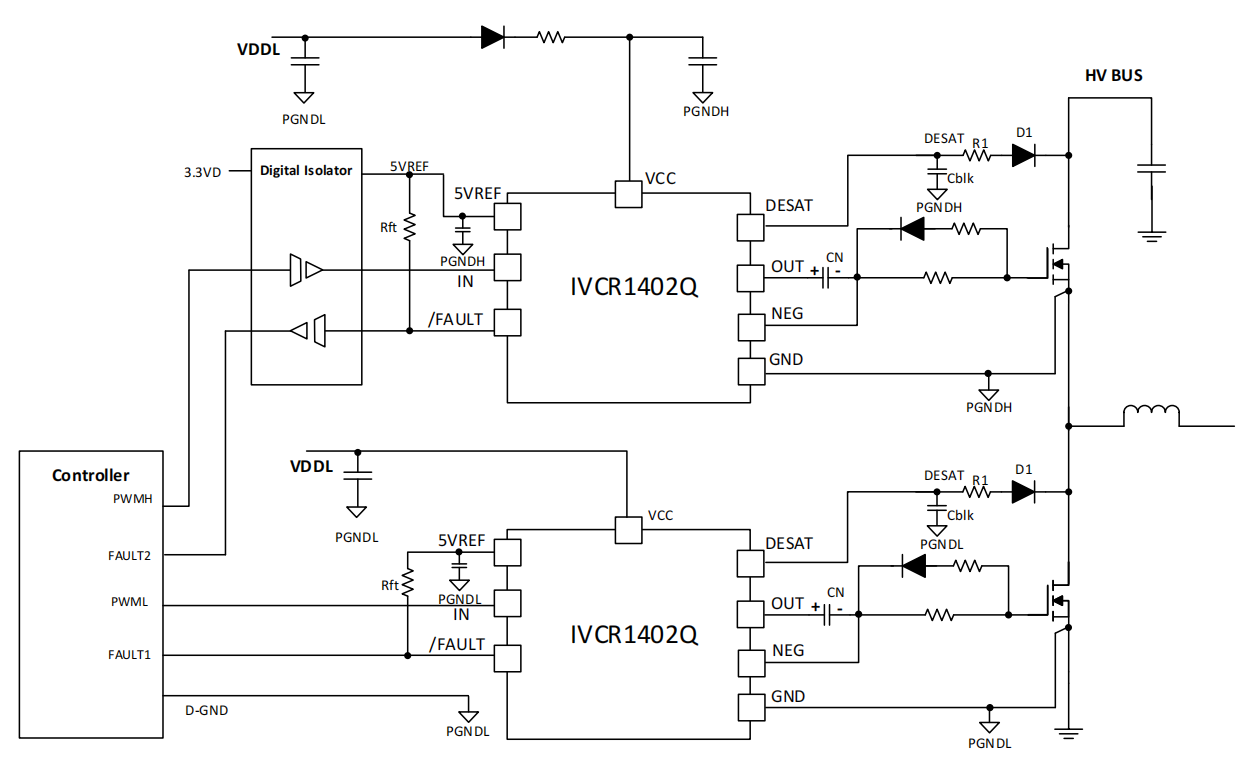
IVCR1402Q is an ideal driver for a compact design. It is a low-side driver. However, with a built-in
negative voltage generator, the driver can be used as a high-side driver without using an isolated bias.
A low-cost bootstrap can then be used instead. Following circuit diagram shows a typical half bridge
driver application.
9 Layout
A good layout is a key step to achieve desired circuit performance. Solid ground is the first to start with.
It is recommended to tie the exposed pad to the driver ground. It is a general rule that capacitors have
a higher priority than resistors for location arrangement. A 1uF and a 0.1uF decoupling capacitors
should be close to VCC pin and grounded to the driver ground plane. Negative voltage capacitor should
locate near to OUT and NEG pins. Blanking capacitor should be close to the driver as well. A small filter
(with10ns time constant) may be needed at the input of IN if the input signal traces have to pass
through some noisy area. Following is a recommended layout.

10 Packaging Information
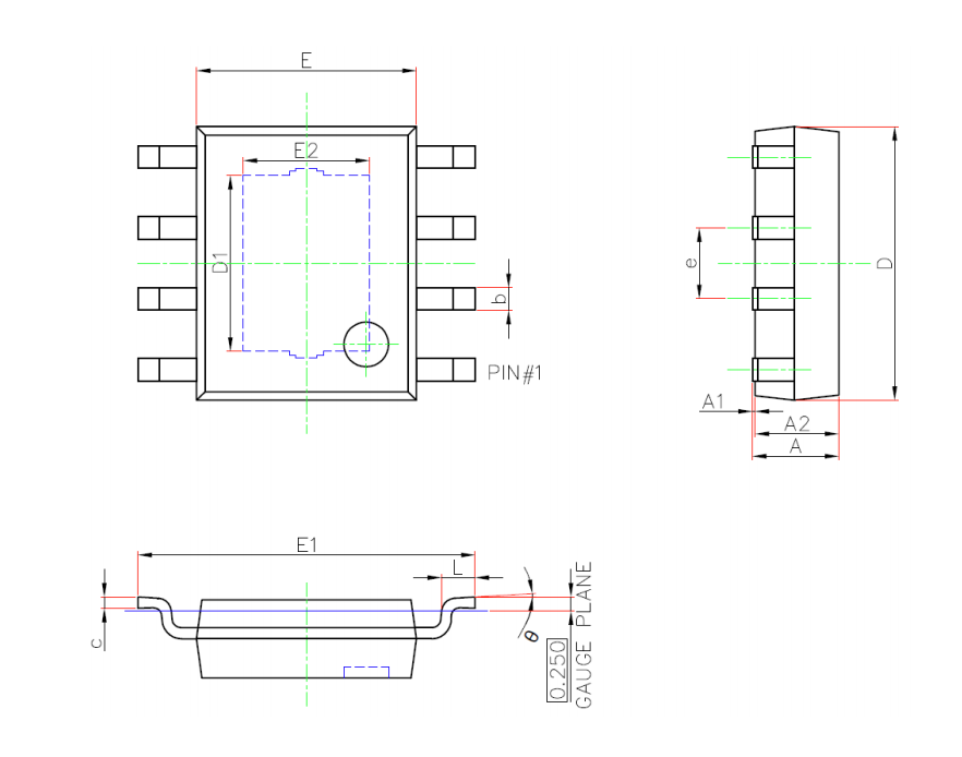
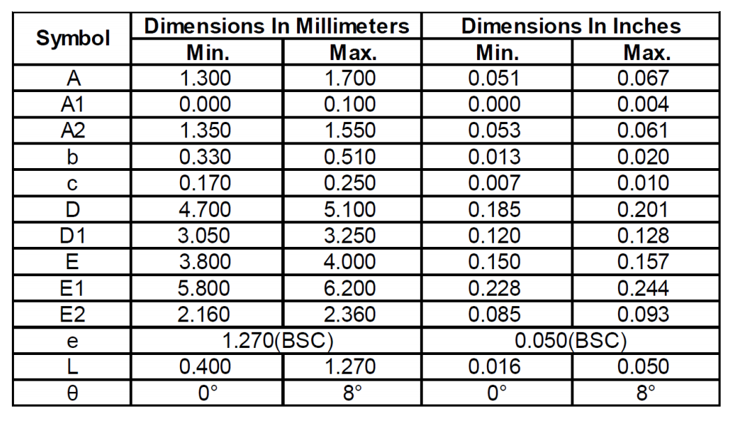
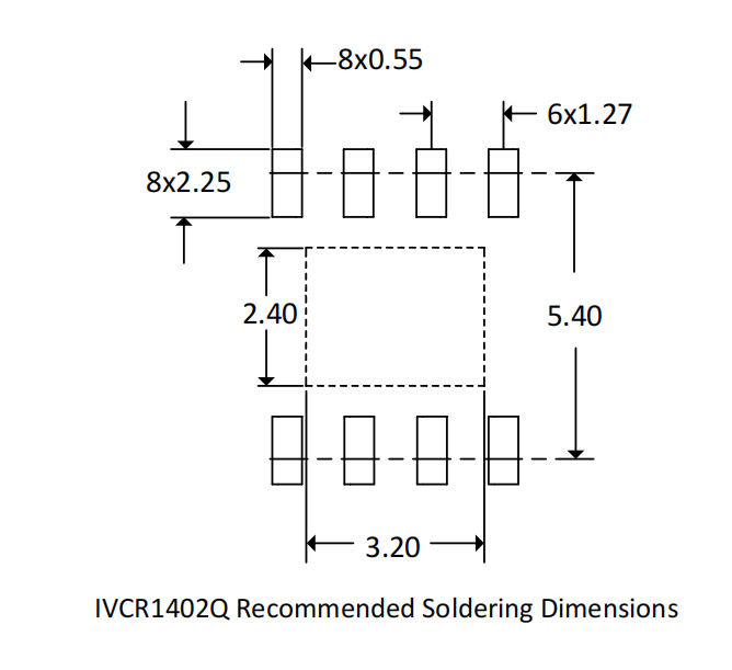
SOIC-8 (EP) Package Dimensions
