Home / Products / Components / SiC MOSFET
| Place of Origin: | Zhejiang |
| Brand Name: | Inventchip Technology |
| Model Number: | IV2Q06025T4Z |
| Certification: | AEC-Q101 |
Features
2 nd Generation SiC MOSFET Technology with
+18V gate drive
High blocking voltage with low on-resistance
High speed switching with low capacitance
High operating junction temperature capability
Very fast and robust intrinsic body diode
Kelvin gate input easing driver circuit design
Applications
Motor drivers
Solar inverters
Automotive DC/DC converters
Automotive compressor inverters
Switch mode power supplies
Outline:
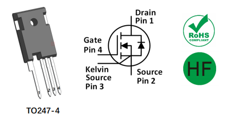
Marking Diagram:

Absolute Maximum Ratings(TC=25°C unless otherwise specified)
| Symbol | Parameter | Value | Unit | Test Conditions | Note |
| VDS | Drain-Source voltage | 650 | V | VGS =0V, ID =100μA | |
| VGSmax (DC) | Maximum DC voltage | -5 to 20 | V | Static (DC) | |
| VGSmax (Spike) | Maximum spike voltage | -10 to 23 | V | Duty cycle<1%, and pulse width<200ns | |
| VGSon | Recommended turn-on voltage | 18±0.5 | V | ||
| VGSoff | Recommended turn-off voltage | -3.5 to -2 | V | ||
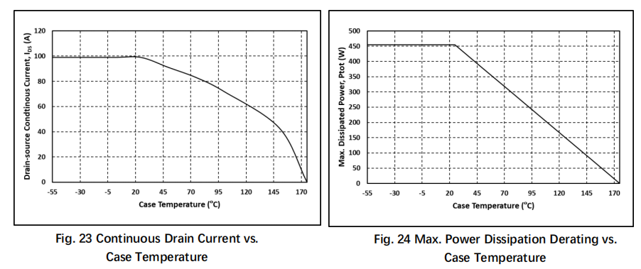
| ID | Drain current (continuous) | 99 | A | VGS =18V, TC =25°C | Fig. 23 |
| 72 | A | VGS =18V, TC =100°C | |||
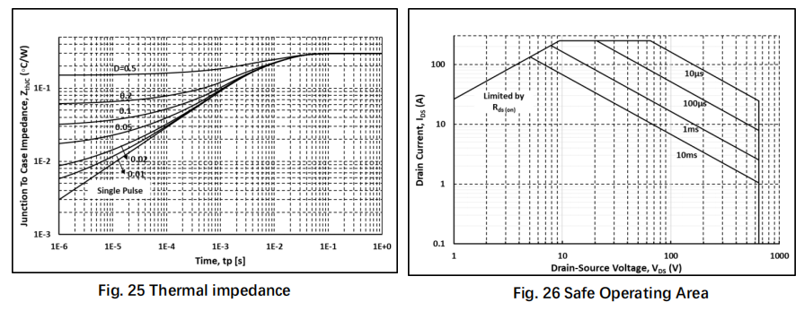
| IDM | Drain current (pulsed) | 247 | A | Pulse width limited by SOA | Fig. 26 |
| PTOT | Total power dissipation | 454 | W | TC =25°C | Fig. 24 |
| Tstg | Storage temperature range | -55 to 175 | °C | ||
| TJ | Operating junctiontemperature | -55 to 175 | °C | ||
| TL | Solder Temperature | 260 | °C | wave soldering only allowed at leads, 1.6mm from case for 10 s |
Thermal Data
| Symbol | Parameter | Value | Unit | Note |
| Rθ(J-C) | Thermal Resistance from Junction to Case | 0.33 | °C/W | Fig. 25 |
Electrical Characteristics(TC =25。C unless otherwise specified)
| Symbol | Parameter | Value | Unit | Test Conditions | Note | ||
| Min. | Typ. | Max. | |||||
| IDSS | Zero gate voltage drain current | 3 | 100 | μA | VDS =650V, VGS =0V | ||
| IGSS | Gate leakage current | ±100 | nA | VDS =0V, VGS = -5~20V | |||
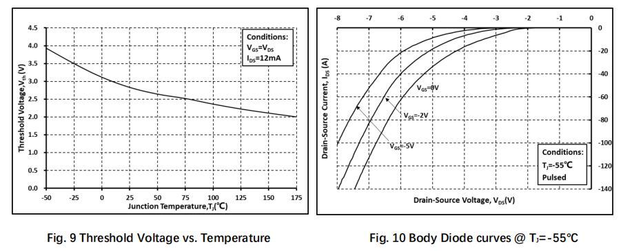
| VTH | Gate threshold voltage | 1.8 | 2.8 | 4.5 | V | VGS=VDS , ID =12mA | Fig. 8, 9 |
| 2.0 | VGS=VDS , ID =12mA @ TJ =175。C | ||||||
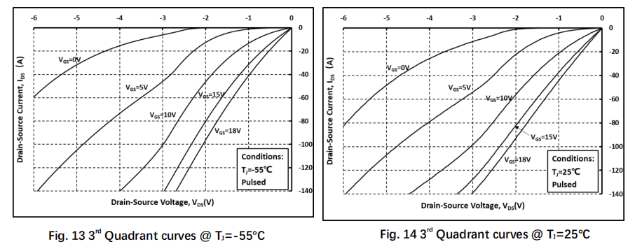
| RON | Static drain-source on- resistance | 25 | 33 | mΩ | VGS =18V, ID =40A @TJ =25。C | Fig. 4, 5, 6, 7 | |
| 38 | mΩ | VGS =18V, ID =40A @TJ =175。C | |||||
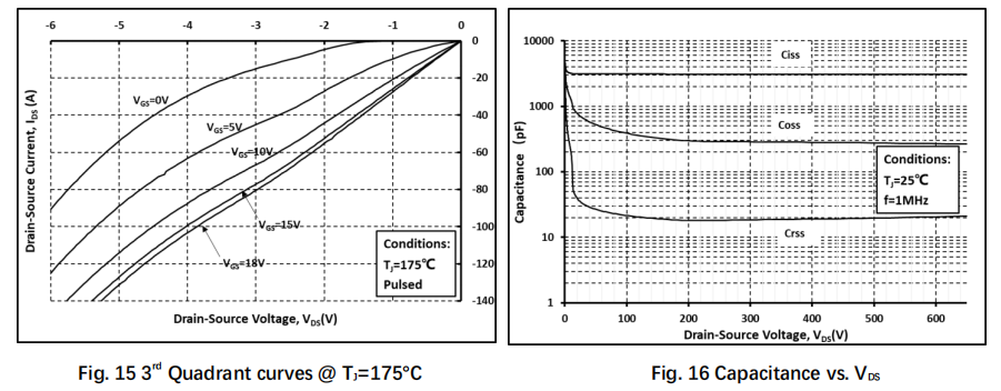
| Ciss | Input capacitance | 3090 | pF | VDS=600V, VGS =0V, f=1MHz, VAC=25mV | Fig. 16 | ||
| Coss | Output capacitance | 251 | pF | ||||
| Crss | Reverse transfer capacitance | 19 | pF | ||||
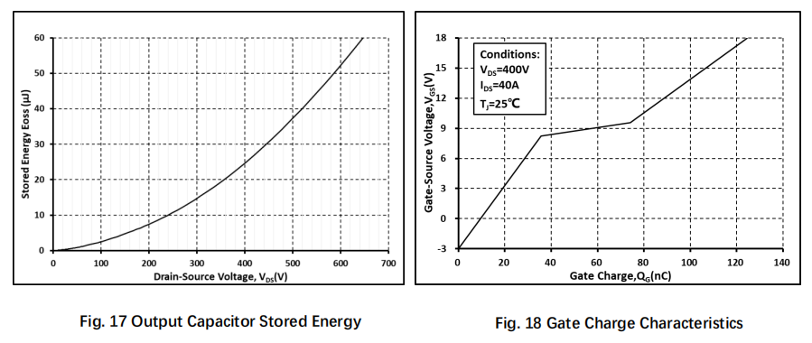
| Eoss | Coss stored energy | 52 | μJ | Fig. 17 | |||
| Qg | Total gate charge | 125 | nC | VDS =400V, ID =40A, VGS =-3 to 18V | Fig. 18 | ||
| Qgs | Gate-source charge | 35.7 | nC | ||||
| Qgd | Gate-drain charge | 38.5 | nC | ||||
| Rg | Gate input resistance | 1.5 | Ω | f=1MHz | |||
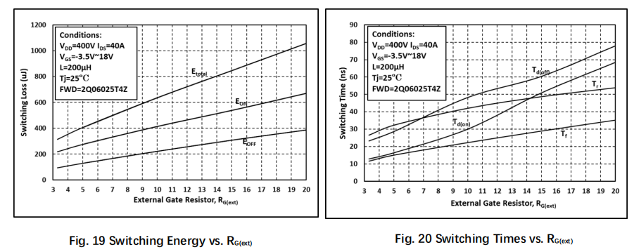
| EON | Turn-on switching energy | 218.8 | μJ | VDS =400V, ID =40A, VGS =-3.5 to 18V, RG(ext) =3.3Ω, L=200μH TJ =25。C | Fig. 19, 20 | ||
| EOFF | Turn-off switching energy | 95.0 | μJ | ||||
| td(on) | Turn-on delay time | 12.9 | ns | ||||
| tr | Rise time | 26.5 | |||||
| td(off) | Turn-off delay time | 23.2 | |||||
| tf | Fall time | 11.7 | |||||
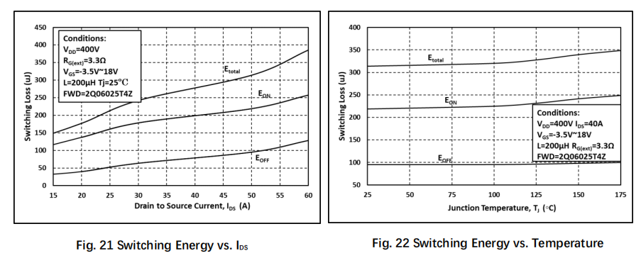
| EON | Turn-on switching energy | 248.5 | μJ | VDS =400V, ID =40A, VGS =-3.5 to 18V, RG(ext) =3.3Ω, L=200μH TJ =175。C | Fig. 22 | ||
| EOFF | Turn-off switching energy | 99.7 | μJ | ||||
Reverse Diode Characteristics(TC =25。C unless otherwise specified)
| Symbol | Parameter | Value | Unit | Test Conditions | Note | ||
| Min. | Typ. | Max. | |||||
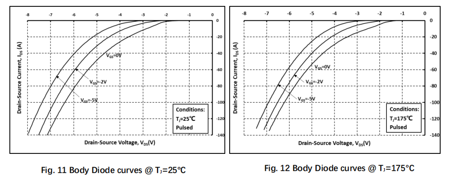
| VSD | Diode forward voltage | 3.7 | V | ISD =20A, VGS =0V | Fig. 10, 11, 12 | ||
| 3.5 | V | ISD =20A, VGS =0V, TJ =175。C | |||||
| trr | Reverse recovery time | 32 | ns | VGS =-3.5V/+18V, ISD =40A, VR =400V, RG(ext) =7.5Ω L=200μH di/dt=3000A/μs | |||
| Qrr | Reverse recovery charge | 195.3 | nC | ||||
| IRRM | Peak reverse recovery current | 20.2 | A | ||||
Typical Performance (curves)
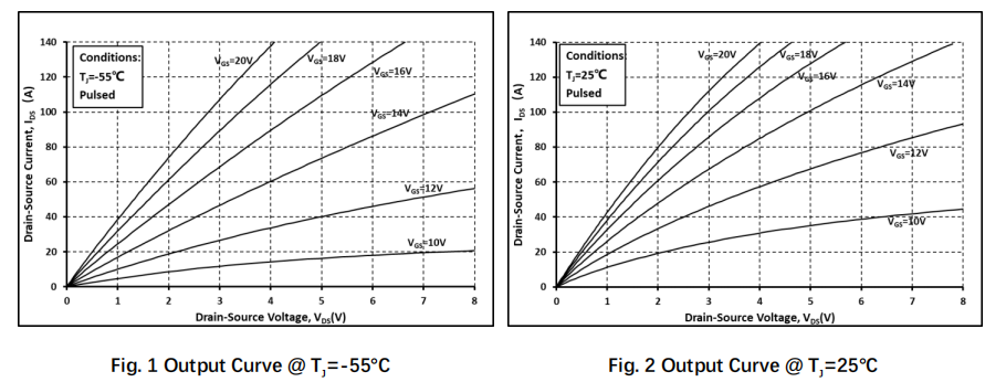
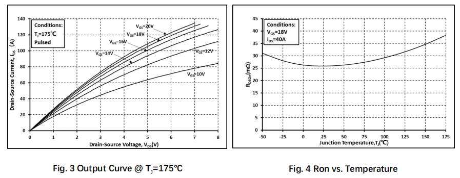
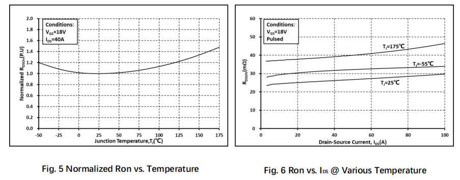

Package Dimensions

Note:
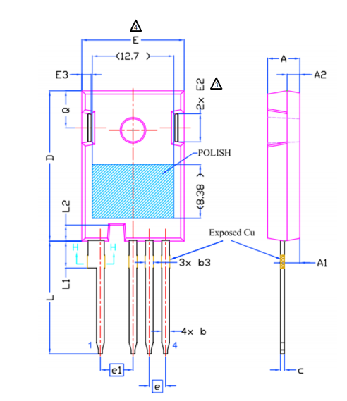
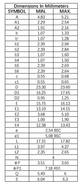
1. Package Reference: JEDEC TO247, Variation AD
2. All Dimensions are in mm
3. Slot Required, Notch May Be Rounded
4. Dimension D&E Do Not Include Mold Flash
5. Subject to Change Without Notice