Home / Products / Components / OSRAM LED
| Place of Origin: | Germany |
| Brand Name: | OSRAM |
| Model Number: | KW HHL532.TK |
| Certification: | AEC-Q102 |
| Minimumpacking Quantity: | 2000 |
| Price: | |
| Packaging Details: | Tape and Reel |
| Delivery Time: | |
| Payment Terms: |
OSLON® Black Flat S
KW HHL532.TK
The OSLON Black Flat S product family meets both, excellent brightness in combination with outstanding luminance.
The SMT device is very stable, durable and can be used with standard SMT processes. A new solder pad layout allows for high reliability and supperior thermal management. The compact chips deliver high light output. The Device is Pin-compatible with LUW HWQP.
Applications
- Static Forward Lighting
Features
- Package: SMD epoxy package
- Chip technology: UX:3
- Typ. Radiation: 120° (Lambertian emitter)
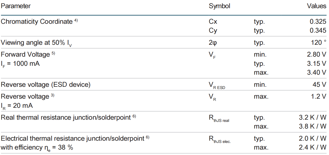
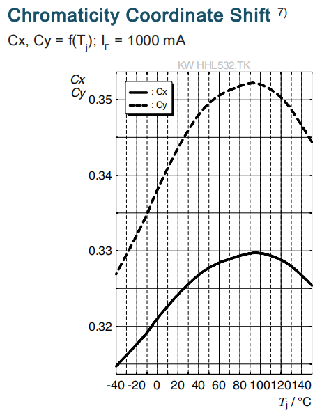
- Color: Cx = 0.325, Cy = 0.345 acc. to CIE 1931 (● ultra white)
- Corrosion Robustness Class: 3B
- Qualifications: AEC-Q102 Qualified
- ESD: 8 kV acc. to ANSI/ESDA/JEDEC JS-001 (HBM, Class 3B)
- Color over angle: Better than passus 3.7.2.1 of supplement proposal 7 to ECE reg. 128
Ordering Information

Maximum Ratings
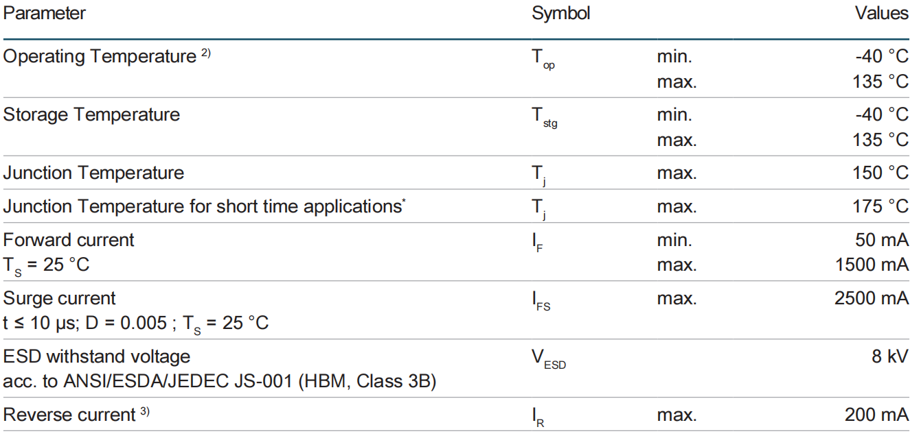
* The median lifetime (L70/B50) for Tj = 175°C is 100h.
Characteristics
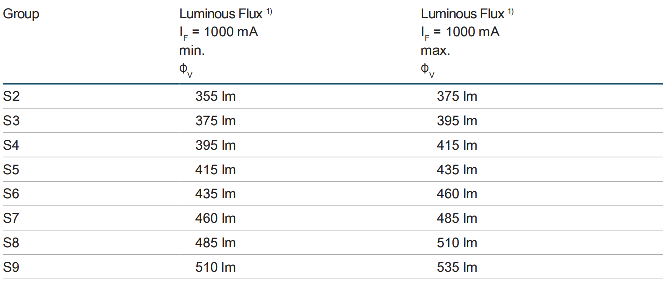
I F = 1000 mA; TS = 25 °C
Brightness Groups
Forward Voltage Groups

Chromaticity Coordinate Group

Chromaticity Coordinate Groups4)
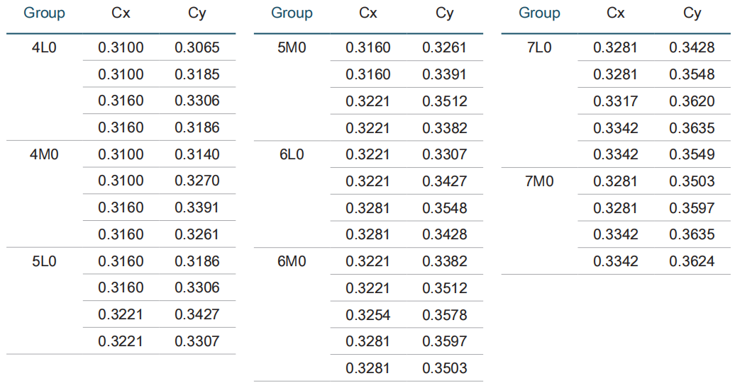
Group Name on Label
Example: S2-4L0-26

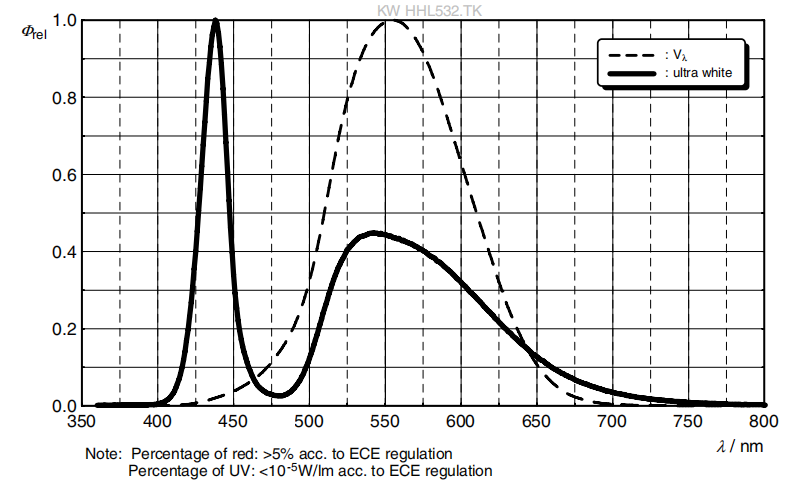
Relative Spectral Emission 7)
Φrel = f (λ); IF = 1000 mA; TJ = 25 °C
Radiation Characteristics7)
I rel = f (ϕ); TJ = 25 °C
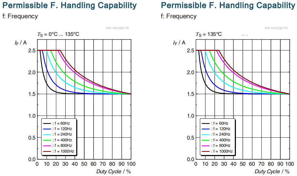
Dimensional Drawing9)
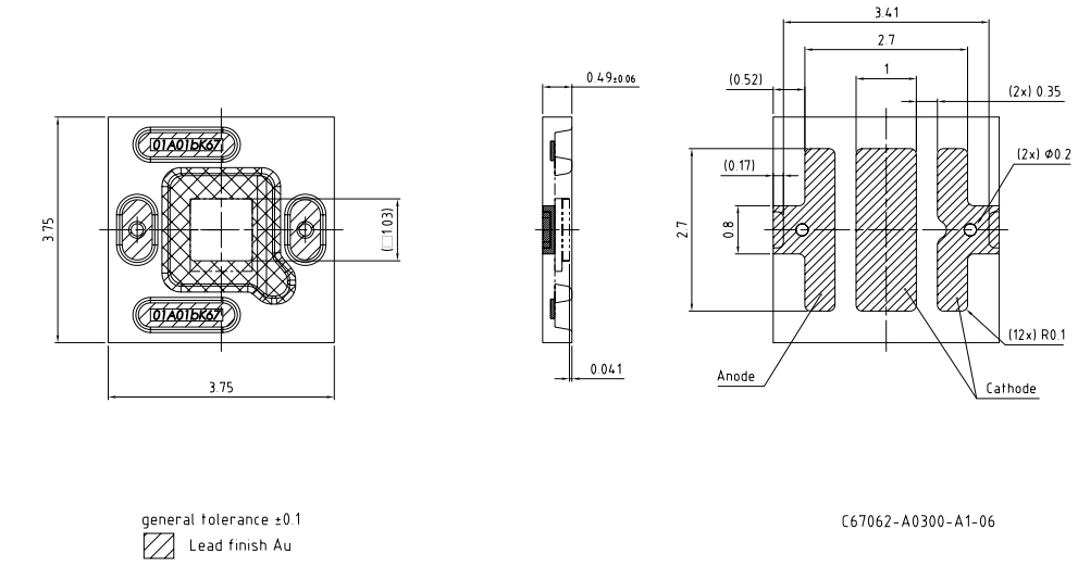
Further Information:
Approximate Weight: 23.0 mg
Corrosion test: Class: 3B
Test condition: 40°C / 90 % RH / 15 ppm H2 S / 14 days (stricter than IEC 60068-2-43)
ESD advice: The device is protected by ESD device which is connected in parallel to the Chip
Electrical Internal Circuit

Recommended Solder Pad9)
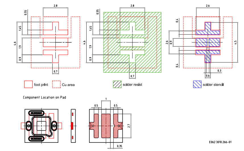
For superior solder joint connectivity results we recommend soldering under standard nitrogen atmosphere. Package not suitable for ultra sonic cleaning. To ensure a high solder joint reliability and to minimize the risk of solder joint cracks, the customer is responsible to evaluate the combination of PCB board and solder paste material for his application.
Reflow Soldering Profile
Product complies to MSL Level 2 acc. to JEDEC J-STD-020E
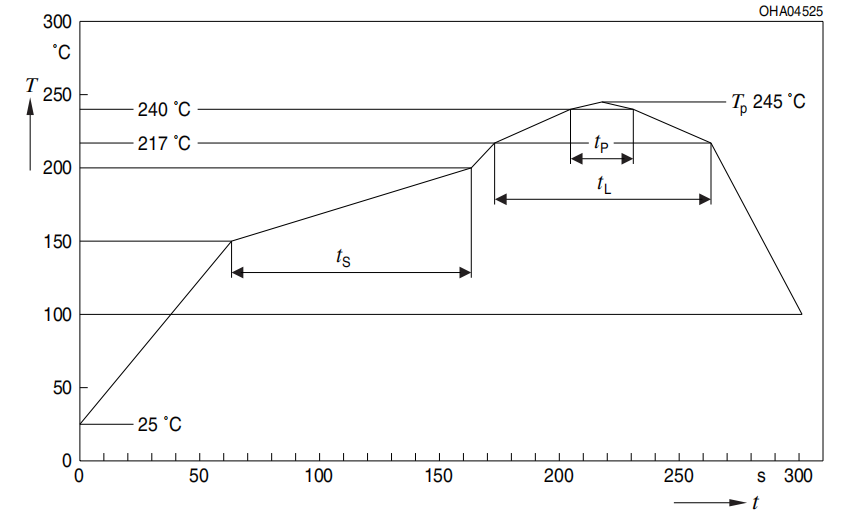

All temperatures refer to the center of the package, measured on the top of the component
* slope calculation DT/Dt: Dt max. 5 s; fulfillment for the whole T-range
Taping9)
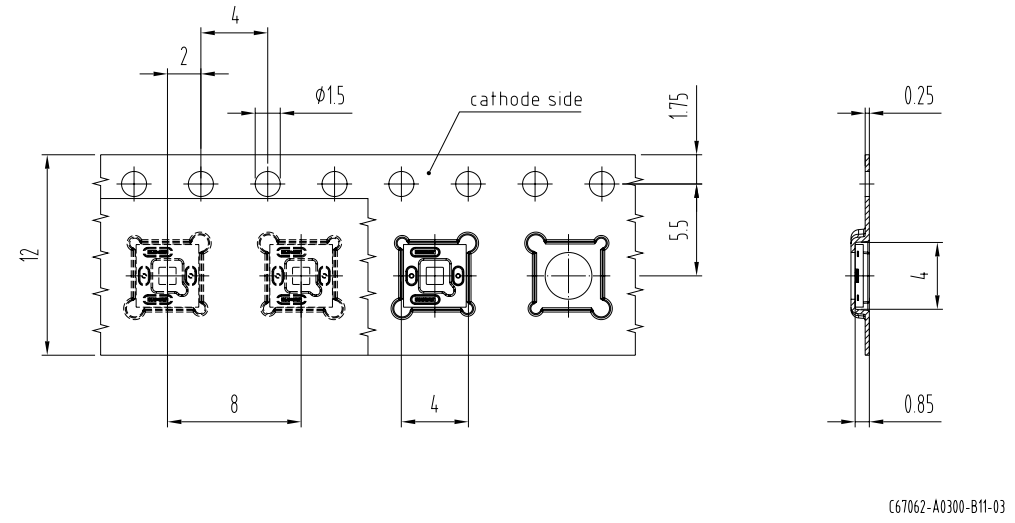
Tape and Reel10)
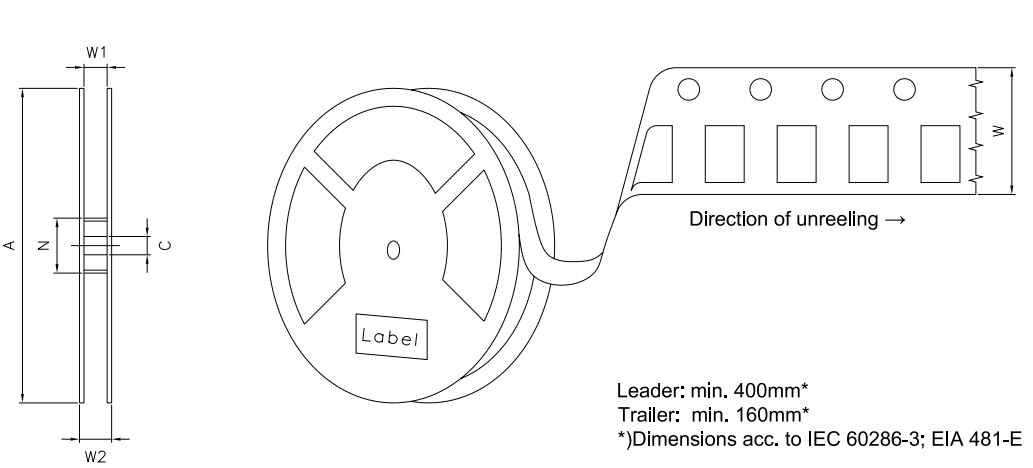
Reel Dimensions

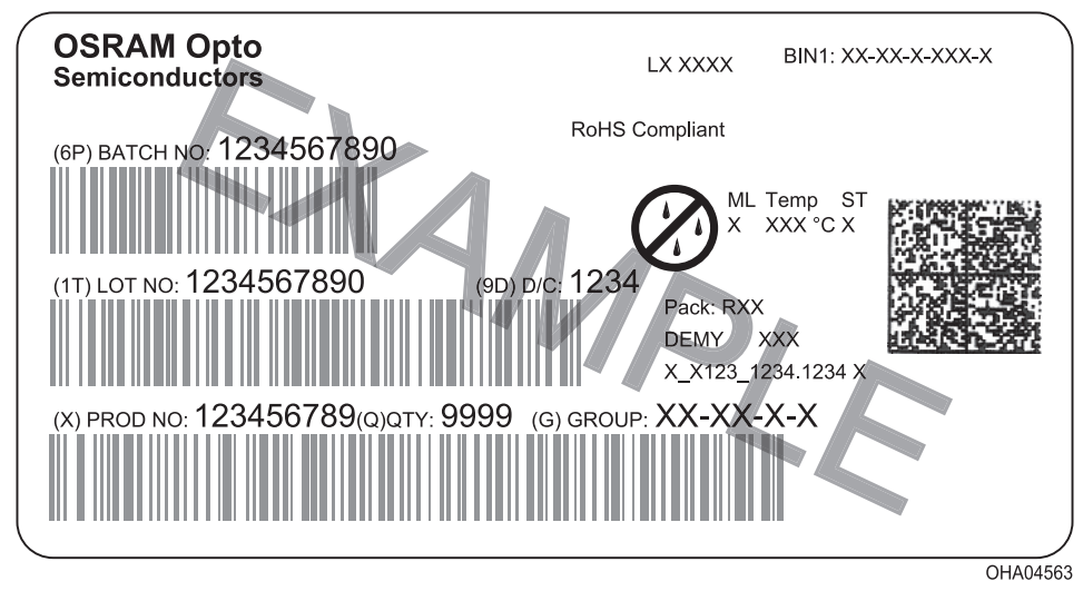
Barcode-Product-Label (BPL)
Dry Packing Process and Materials9)
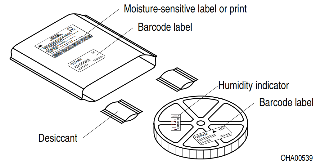
Moisture-sensitive product is packed in a dry bag containing desiccant and a humidity card according JEDEC-STD-033.
TypeDesignation System
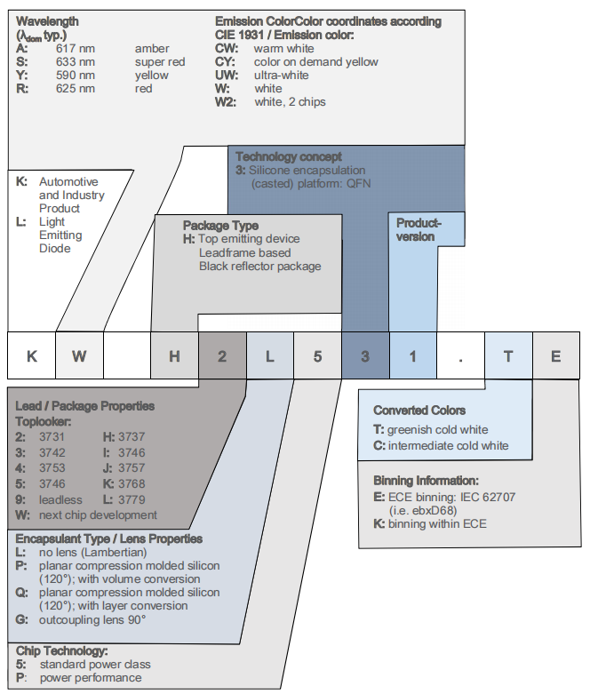
Notes
The evaluation of eye safety occurs according to the standard IEC 62471:2006 (photo biological safety of lamps and lamp systems). Within the risk grouping system of this IEC standard, the device specified in this data sheet fall into the class moderate risk (exposure time 0.25 s). Under real circumstances (for exposure time, conditions of the eye pupils, observation distance), it is assumed that no endangerment to the eye exists from these devices. As a matter of principle, however, it should be mentioned that intense light sources have a high secondary exposure potential due to their blinding effect. When looking at bright light sources(e.g. headlights), temporary reduction in visual acuity and afterimages can occur, leading to irritation, annoyance, visual impairment, and even accidents, depending on the situation.
Subcomponents of this device contain, in addition to other substances, metal filled materials including silver.Metal filled materials can be affected by environments that contain traces of aggressive substances. Therefore, we recommend that customers minimize device exposure to aggressive substances during storage,production, and use. Devices that showed visible discoloration when tested using the described tests above did show no performance deviations within failure limits during the stated test duration. Respective failure limits are described in the IEC60810.
For further application related information please visitwww.osram-os.com/appnotes
Disclaimer
Attention please!
The information describes the type of component and shall not be considered as assured characteristics.
Terms of delivery and rights to change design reserved. Due to technical requirements components may contain dangerous substances.
For information on the types in question please contact our Sales Organization.
If printed or downloaded, please find the latest version on our website.
Packing
Please use the recycling operators known to you. We can also help you – get in touch with your nearest
sales office. By agreement we will take packing material back, if it is sorted. You must bear the costs of
transport. For packing material that is returned to us unsorted or which we are not obliged to accept, we shall have to invoice you for any costs incurred.
Product and functional safety devices/applications or medical devices/applications
Our components are not developed, constructed or tested for the application as safety relevant component or for the application in medical devices.
Our products are not qualified at module and system level for such application.
In case buyer – or customer supplied by buyer – considers using our components in product safety devices/applications or medical devices/applications, buyer and/or customer has to inform our local sales partner immediately and we and buyer and /or customer will analyze and coordinate the customer-specific request between us and buyer and/or customer.
Glossary
1)Brightness: Brightness values are measured during a current pulse of typically 1 ms, with an internal
reproducibility of ±8 % and an expanded uncertainty of ±11 % (acc. to GUM with a coverage factor of
k = 3).
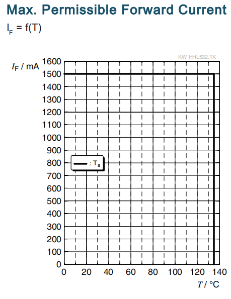
2)Operating Temperature:The Operating Temperatur Top is referenced to the Solderpoint Ts of this device. Proper current derating must be observed to maintain junction temperature below the maximum.
3)Reverse Operation: This product is intended to be operated applying a forward current within the
specified range. Applying any continuous reverse bias or forward bias below the voltage range of light
emission shall be avoided because it may cause migration which can change the electro-optical char
acteristics or damage the LED.
4)Chromaticity coordinate groups:Chromaticity coordinates are measured during a current pulse of
typically 1 ms, with an internal reproducibility of ±0.005 and an expanded uncertainty of ±0.01 (acc. to
GUM with a coverage factor of k = 3).
5)Forward Voltage: The forward voltage is measured during a current pulse of typically 1 ms, with an
internal reproducibility of ±0.05 V and an expanded uncertainty of ±0.1 V (acc. to GUM with a coverage
factor of k = 3).
6)Thermal Resistance: Rth max is based on statistic values (6σ).
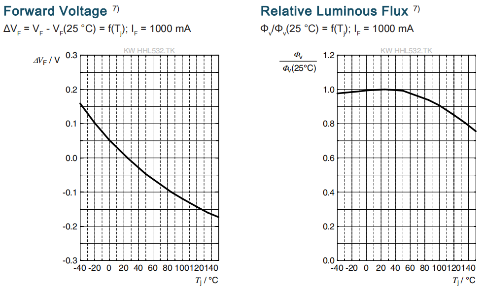
7)Typical Values:Due to the special conditions of the manufacturing processes of semiconductor devices, the typical data or calculated correlations of technical parameters can only reflect statistical figures.These do not necessarily correspond to the actual parameters of each single product, which could differ from the typical data and calculated correlations or the typical characteristic line. If requested, e.g.because of technical improvements, these typ. data will be changed without any further notice.
8)Characteristic curve: In the range where the line of the graph is broken, you must expect higher differences between single devices within one packing unit.
9)Tolerance of Measure: Unless otherwise noted in drawing, tolerances are specified with ±0.1 and
dimensions are specified in mm.
10)Tape and Reel: All dimensions and tolerances are specified acc. IEC 60286-3 and specified in mm.
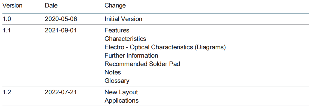
Revision History
