Home / Products / Components / SiC SBD
| Place of Origin: | Zhejiang |
| Brand Name: | Inventchip Technology |
| Model Number: | IV1D12040U3Z |
| Certification: | AEC-Q101 qualified |
| Minimumpacking Quantity: | 450PCS |
| Price: | |
| Packaging Details: | |
| Delivery Time: | |
| Payment Terms: | |
| Supply Ability: |
Features
Max Junction Temperature 175°C
High Surge Current Capacity
Zero Reverse Recovery Current
Zero Forward Recovery Voltage
High-Frequency Operation
Temperature independent switching behavior
Positive Temperature Coefficient on VF
AEC-Q101 qualified
Applications
Automotive Inverter Free Wheeling Diodes
EV Charger Piles
Vienna 3-Phase PFC
Solar Power Boost
Switch Mode Power Supplies
Outline
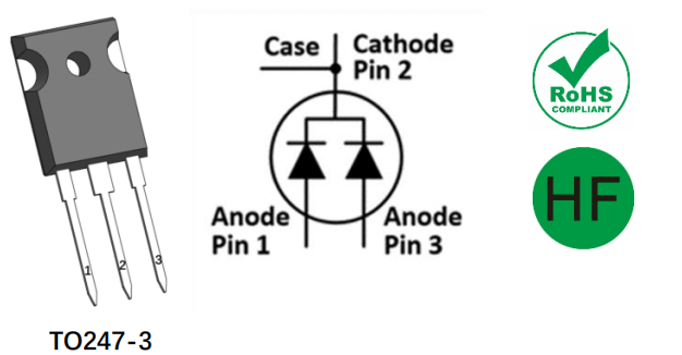
Marking Diagram

Absolute Maximum Ratings(Tc=25°C unless otherwise specified)
| Symbol | Parameter | Value | Unit |
| VRRM | Reverse voltage (repetitive peak) | 1200 | V |
| VDC | DC blocking voltage | 1200 | V |
| IF | Forward current (continuous) @Tc=25°C | 54* | A |
| Forward current (continuous) @Tc=135°C | 28* | A | |
| Forward current (continuous) @Tc=151°C | 20* | A | |
| IFSM | Surge non-repetitive forward current sine halfwave @Tc=25°C tp=10ms | 140* | A |
| IFRM | Surge repetitive forward current (Freq=0.1Hz, 100cycles) sine halfwave @Tamb =25°C tp=10ms | 115* | A |
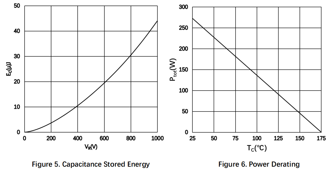
| Ptot | Total power dissipation @ Tc=25°C | 272* | W |
| Total power dissipation @ Tc=150°C | 45* | ||
| I2t value @Tc=25°C tp=10ms | 98* | A2s | |
| Tstg | Storage temperature range | -55 to 175 | °C |
| Tj | Operating junction temperature range | -55 to 175 | °C |
*Per Leg
Stresses exceeding those listed in the Maximum Ratings table may damage the device. If any of these limits are exceeded, device
functionality should not be assumed, damage may occur and reliability may be affected.
Electrical Characteristics
| Symbol | Parameter | Typ. | Max. | Unit | Test Conditions | Note |
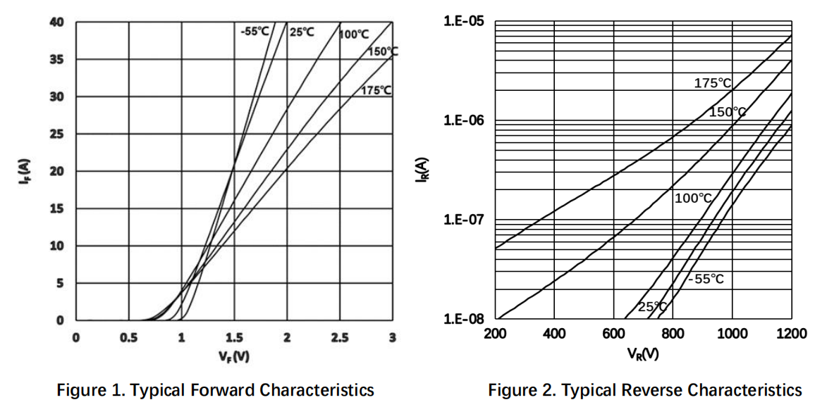
| VF | Forward Voltage | 1.48* | 1.8* | V | IF = 20 A TJ =25°C | Fig. 1 |
| 2.1* | 3.0* | IF = 20 A TJ =175°C | ||||
| IR | Reverse Current | 10* | 200* | μA | VR = 1200 V TJ =25°C | Fig. 2 |
| 45* | 800* | VR = 1200 V TJ =175°C | ||||
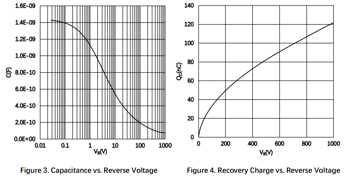
| C | Total Capacitance | 1114* | pF | VR = 1 V, TJ = 25°C, f = 1 MHz | Fig. 3 | |
| 100* | VR = 400 V, TJ = 25˚C, f = 1 MHz | |||||
| 77* | VR = 800 V, TJ = 25˚C, f = 1 MHz | |||||
| QC | Total Capacitive Charge | 107* | nC | VR = 800 V, TJ = 25°C, Qc = C(v)dv | Fig. 4 | |
| EC | Capacitance Stored Energy | 31* | μJ | VR = 800 V, TJ = 25°C, Ec = C(v) ⋅vdv | Fig. 5 |
*Per Leg
Thermal Characteristics (Per Leg)
| Symbol | Parameter | Typ. | Unit | Note |
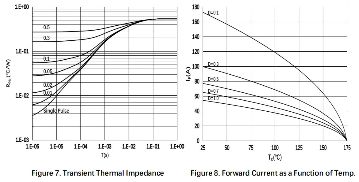
| Rth(j-c) | Thermal Resistance from Junction to Case | 0.55 | °C/W | Fig.7 |
Typical Performance (Per Leg)
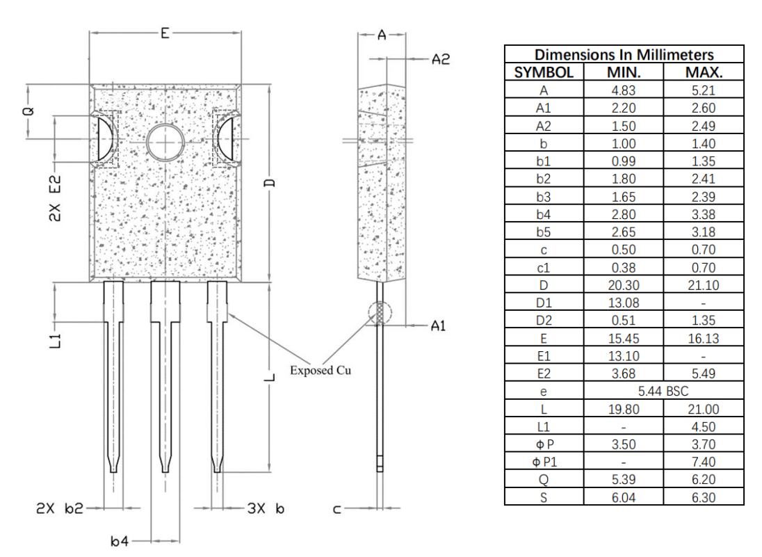
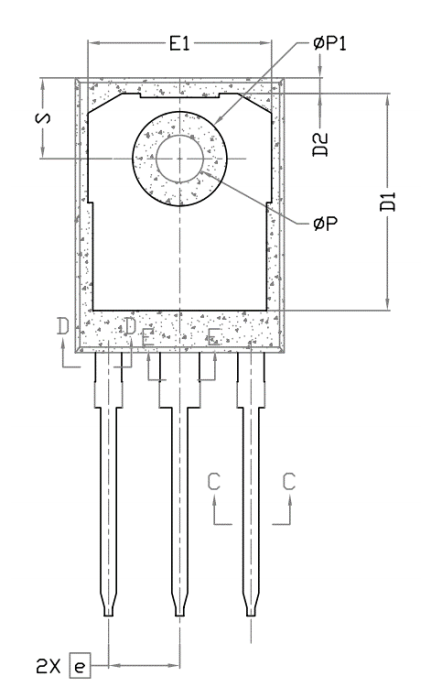
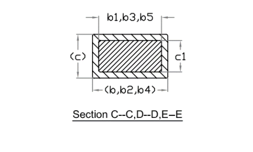
Package Dimensions
Note:
1. Package Reference: JEDEC TO247, Variation AD
2. All Dimensions are in mm
3. Slot Required, Notch May Be Rounded or Rectangular
4. Dimension D&E Do Not Include Mold Flash
5. Subject to Change Without Notice