Home / Products / Components / SiC Module
| Place of Origin: | Zhejiang |
| Brand Name: | Inventchip Technology |
| Model Number: | IV1B12025HC1L |
| Certification: | AEC-Q101 |
Features
High blocking voltage with low on-resistance
High speed switching with low capacitance
High operating junction temperature capability
Very fast and robust intrinsic body diode
Applications
Solar applications
UPS system
Motor drivers
High voltage DC/DC converters
Package
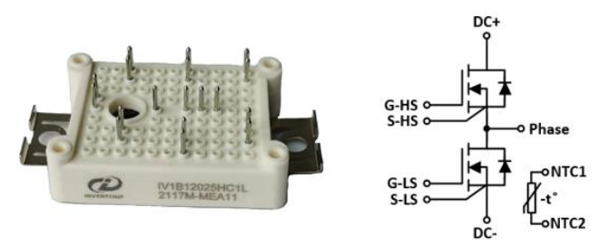

Absolute Maximum Ratings(TC=25°C unless otherwise specified)
| Symbol | Parameter | Value | Unit | Test Conditions | Note |
| VDS | Drain-Source voltage | 1200 | V | VGS =0V, ID =200μA | |
| VGSmax (DC) | Maximum DC voltage | -5 to 22 | V | Static (DC) | |
| VGSmax (Spike) | Maximum spike voltage | -10 to 25 | V | <1% duty cycle, and pulse width<200ns | |
| VGSon | Recommended turn -on voltage | 20±0.5 | V | ||
| VGSoff | Recommended turn -off voltage | -3.5 to -2 | V | ||
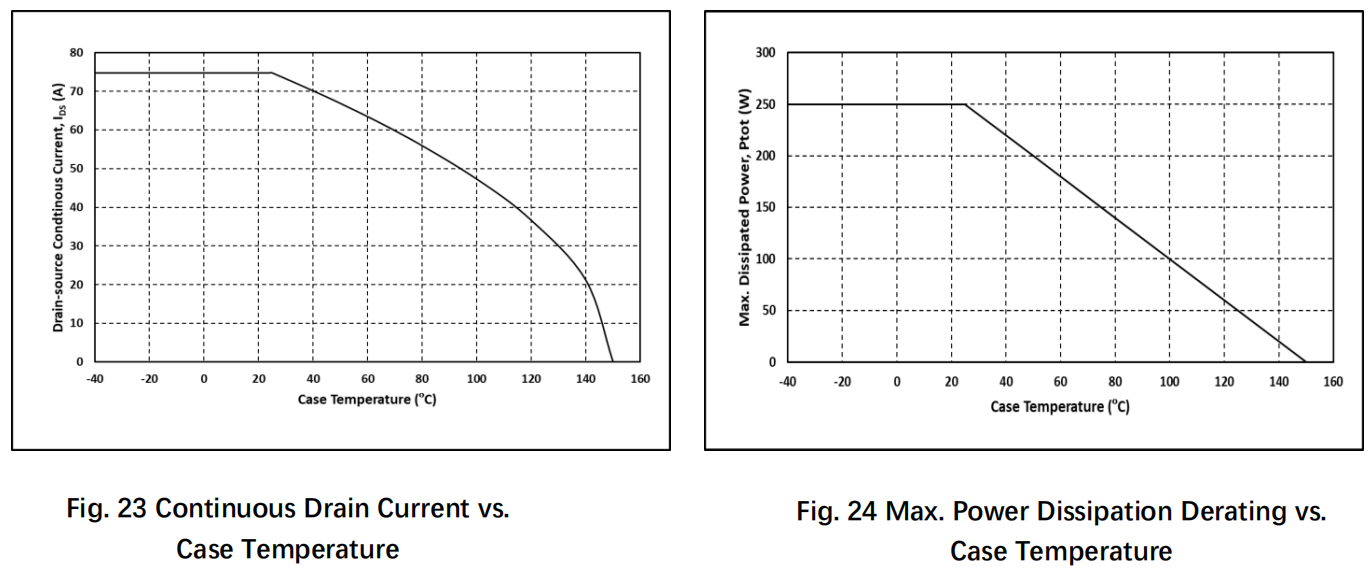
| ID | Drain current (continuous) | 74 | A | VGS =20V, TC =25°C | |
| 50 | A | VGS =20V, TC =94°C | |||
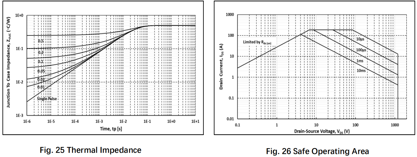
| IDM | Drain current (pulsed) | 185 | A | Pulse width limited by SOA | Fig.26 |
| PTOT | Total power dissipation | 250 | W | TC =25°C | Fig.24 |
| Tstg | Storage temperature range | -40 to 150 | °C | ||
| TJ | Maximum virtual junction temperature under switching conditions | -40 to 150 | °C | Operation | |
| -55 to 175 | °C | Intermittent with reduced life |
Thermal Data
| Symbol | Parameter | Value | Unit | Note |
| Rθ(J-C) | Thermal Resistance from Junction to Case | 0.5 | °C/W | Fig.25 |
Electrical Characteristics(TC=25°C unless otherwise specified)
| Symbol | Parametr | Value | Unit | Test Conditions | Note | ||
| Min. | Typ. | Max. | |||||
| IDSS | Zero gate voltage drain current | 10 | 200 | μA | VDS =1200V, VGS =0V | ||
| IGSS | Gate leakage current | 2 | ±200 | nA | VDS =0V, VGS = -5~20V | ||
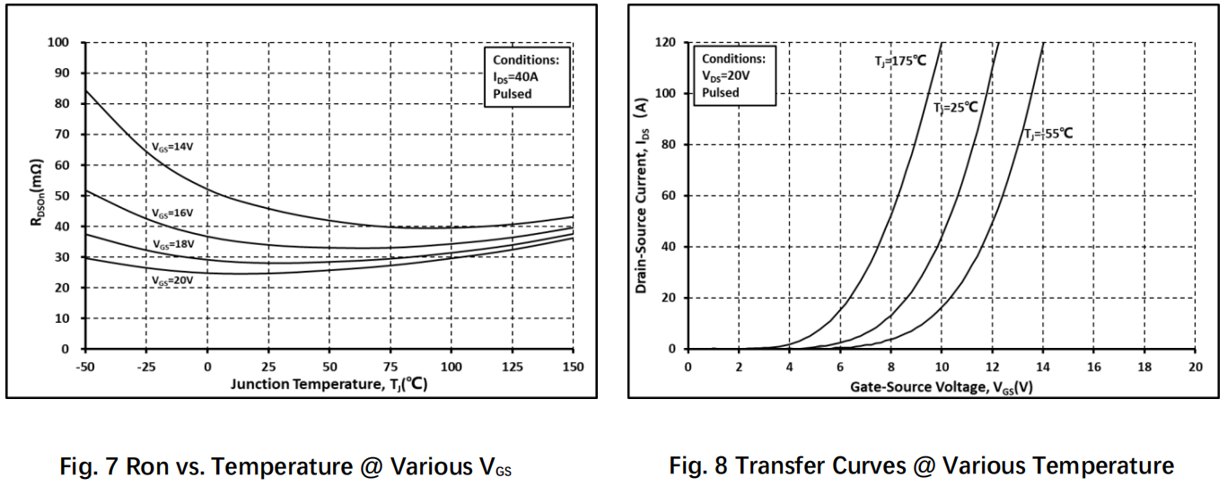
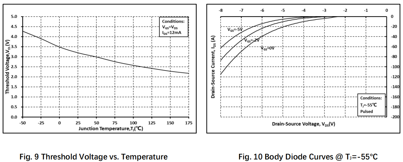
| VTH | Gate threshold voltage | 3.2 | V | VGS=VDS , ID =12mA | Fig.9 | ||
| 2.3 | VGS=VDS , ID =12mA @ TC =150。C | ||||||
| RON | Static drain-source on - resistance | 25 | 33 | mΩ | VGS =20V, ID =40A @TJ =25。C | Fig.4-7 | |
| 36 | mΩ | VGS =20V, ID =40A @TJ =150。C | |||||
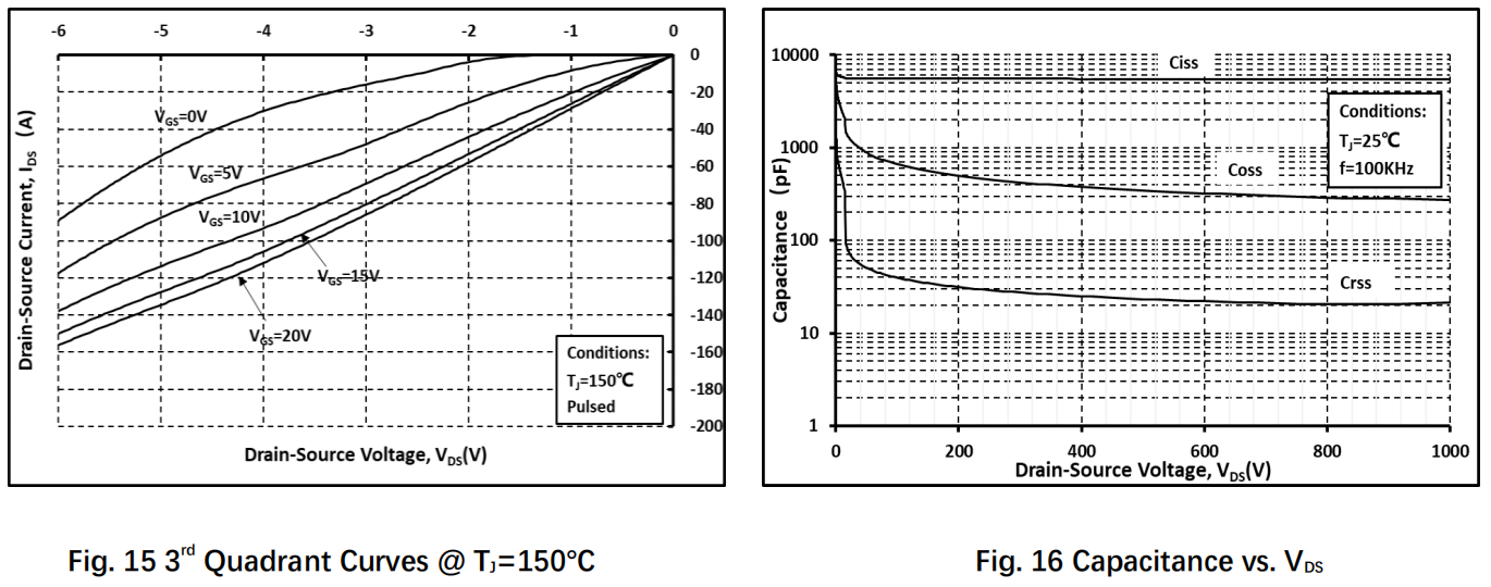
| Ciss | Input capacitance | 5.5 | nF | VDS=800V, VGS =0V, f=100kHZ , VAC =25mV | Fig.16 | ||
| Coss | Output capacitance | 285 | pF | ||||
| Crss | Reverse transfer capacitance | 20 | pF | ||||
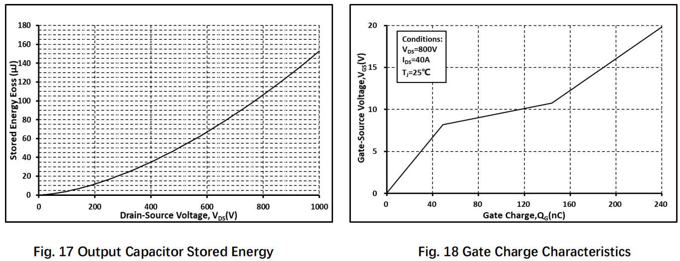
| Eoss | Coss stored energy | 105 | μJ | Fig.17 | |||
| Qg | Total gate charge | 240 | nC | VDS =800V, ID =40A, VGS =-5 to 20V | Fig.18 | ||
| Qgs | Gate-source charge | 50 | nC | ||||
| Qgd | Gate-drain charge | 96 | nC | ||||
| Rg | Gate input resistance | 1.4 | Ω | f=100kHZ | |||
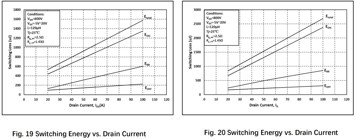
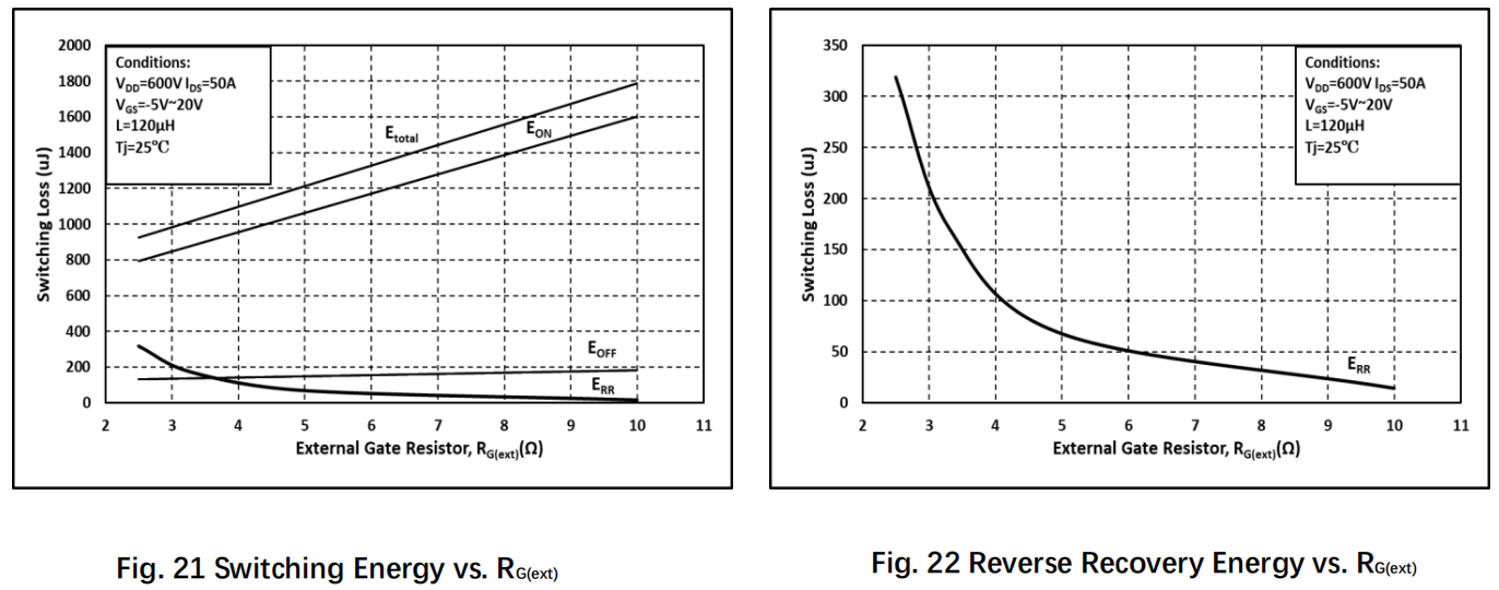
| EON | Turn-on switching energy | 795 | μJ | VDS =600V, ID =50A, VGS=-5 to 20V, RG(ext)on/ RG(ext)off =2.5Ω/1.43Ω, L=120μH | Fig.19-22 | ||
| EOFF | Turn-off switching energy | 135 | μJ | ||||
| td(on) | Turn-on delay time | 15 | ns | ||||
| tr | Rise time | 4.1 | |||||
| td(off) | Turn-off delay time | 24 | |||||
| tf | Fall time | 17 | |||||
| LsCE | Stray inductance | 8.8 | nH | ||||
Reverse Diode Characteristics(TC=25°C unless otherwise specified)
| Symbol | Parameter | Value | Unit | Test Conditions | Note | ||
| Min. | Typ. | Max. | |||||
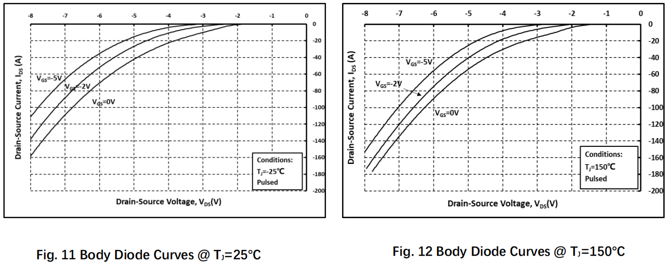
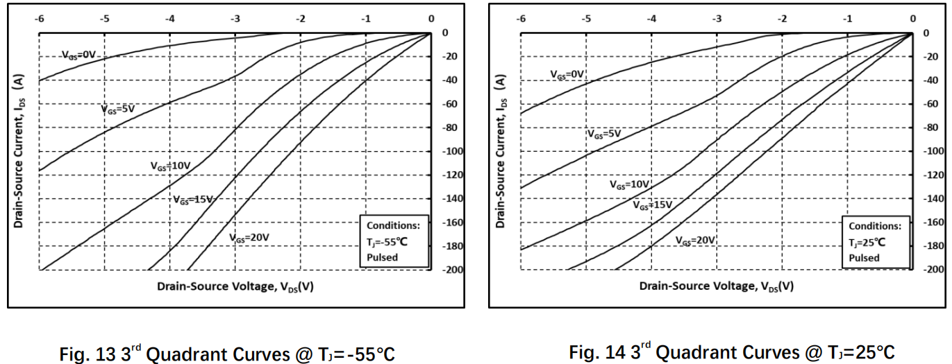
| VSD | Diode forward voltage | 4.9 | V | ISD =40A, VGS =0V | Fig.10- 12 | ||
| 4.5 | V | ISD =40A, VGS =0V, TJ =150°C | |||||
| trr | Reverse recovery time | 18 | ns | VGS =-5V/+20V, ISD =50A, VR =600V, di/dt=14.29A/ns, RG(ext) =2.5Ω, L=120μH | |||
| Qrr | Reverse recovery charge | 1068 | nC | ||||
| IRRM | Peak reverse recovery current | 96.3 | A | ||||
NTC Thermistor Characteristics
| Symbol | Parameter | Value | Unit | Test Conditions | Note | ||
| Min. | Typ. | Max. | |||||
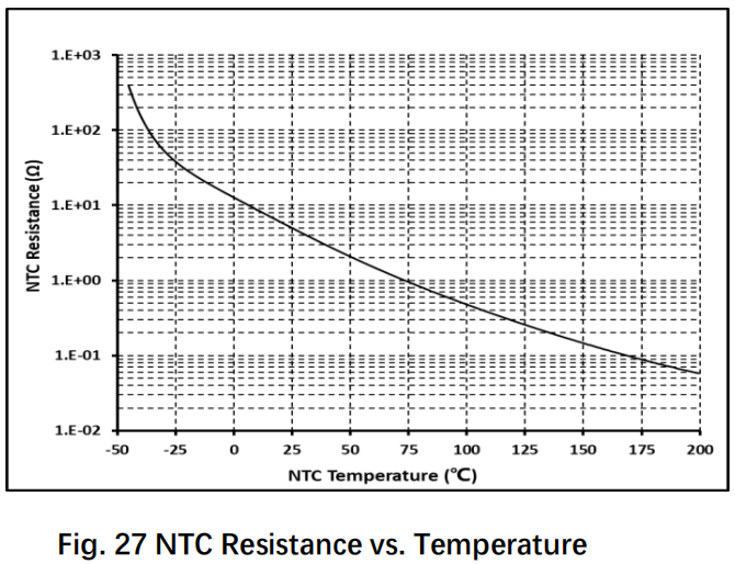
| RNTC | Rated Resistance | 5 | kΩ | TNTC =25℃ | Fig.27 | ||
| ΔR/R | Resistance Tolerance at 25℃ | -5 | 5 | % | |||
| β25/50 | Beta Value | 3380 | K | ±1% | |||
| Pmax | Power Dissipation | 5 | mW | ||||
Typical Performance (curves)
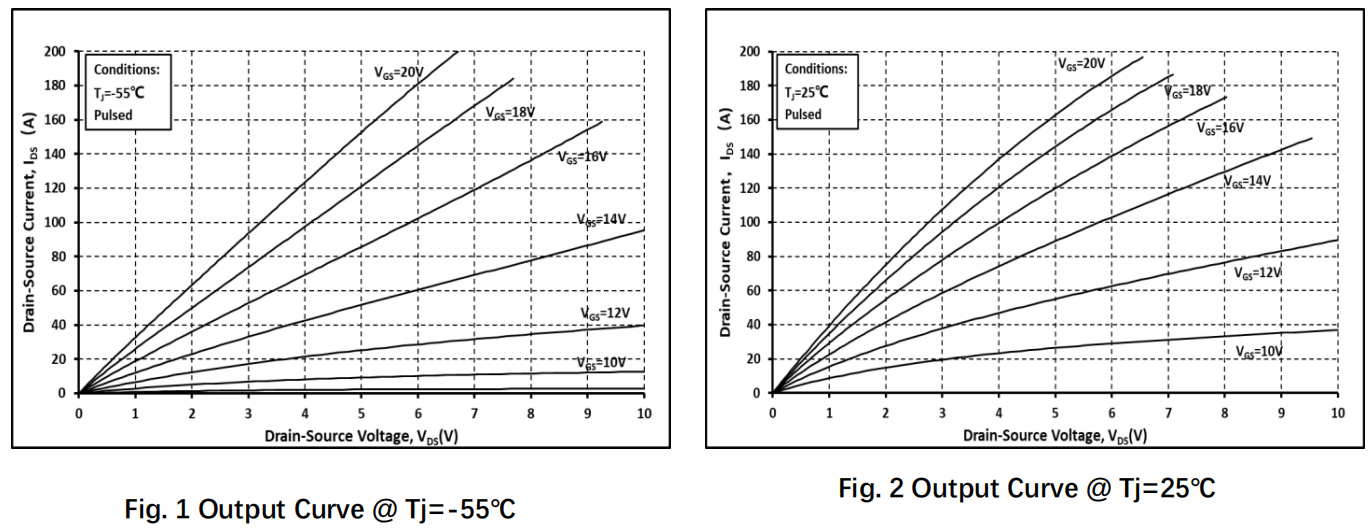
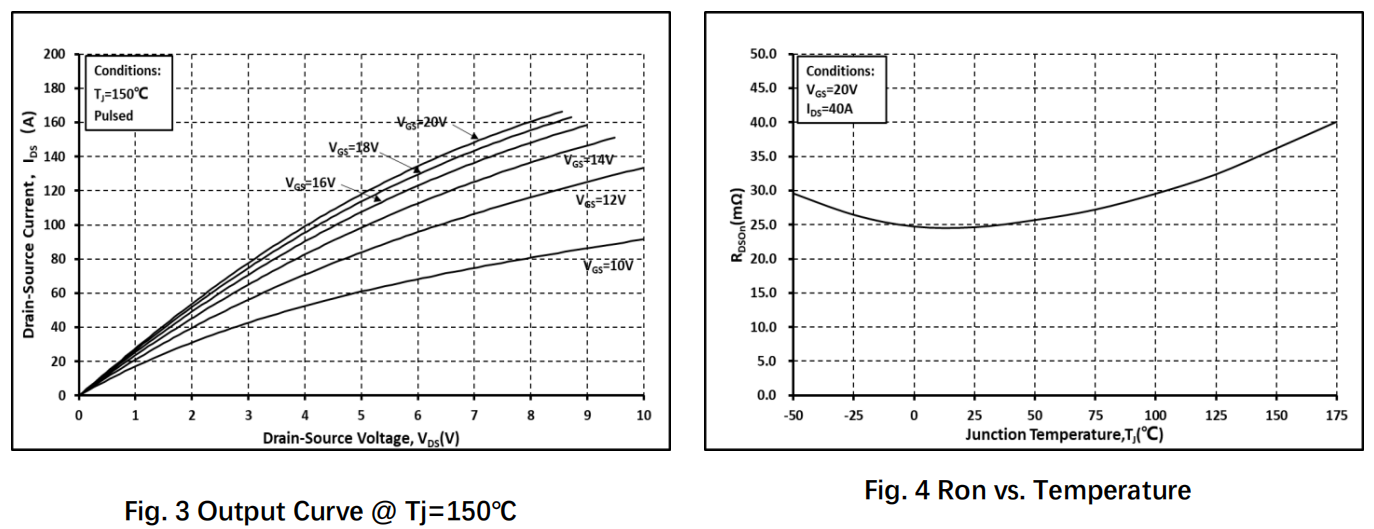
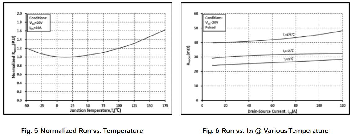
Package Dimensions (mm)
Notes
For further information please contact IVCT’s Sales Office.
Copyright©2022 InventChip Technology Co., Ltd. All rights reserved.
The information in this document is subject to change without notice.
Related Links
http://www.inventchip.com.cn