Home / Products / Components / SiC MOSFET
| Place of Origin: | Zhejiang |
| Brand Name: | Inventchip Technology |
| Model Number: | IV2Q12160T4Z |
| Certification: | AEC-Q101 |
| Minimum Order Quantity: | 450PCS |
| Price: | |
| Packaging Details: | |
| Delivery Time: | |
| Payment Terms: | |
| Supply Ability: |
Features
2 nd Generation SiC MOSFET Technology with +18V gate drive
High blocking voltage with low on-resistance
High speed switching with low capacitance
High operating junction temperature capability
Very fast and robust intrinsic body diode
Kelvin gate input easing driver circuit design
Applications
Automotive DC/DC converters
On-board chargers
Solar inverters
Motor drivers
Automotive compressor inverters
Switch mode power supplies
Outline:
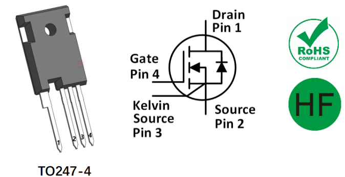
Marking Diagram:

Absolute Maximum Ratings(TC=25°C unless otherwise specified)
| Symbol | Parameter | Value | Unit | Test Conditions | Note |
| VDS | Drain-Source voltage | 1200 | V | VGS =0V, ID =100μA | |
| VGSmax (DC) | Maximum DC voltage | -5 to 20 | V | Static (DC) | |
| VGSmax (Spike) | Maximum spike voltage | -10 to 23 | V | Duty cycle<1%, and pulse width<200ns | |
| VGSon | Recommended turn-on voltage | 18±0.5 | V | ||
| VGSoff | Recommended turn-off voltage | -3.5 to -2 | V | ||
| ID | Drain current (continuous) | 19 | A | VGS =18V, TC =25°C | Fig. 23 |
| 14 | A | VGS =18V, TC =100°C | |||
| IDM | Drain current (pulsed) | 47 | A | Pulse width limited by SOA | Fig. 26 |
| PTOT | Total power dissipation | 136 | W | TC =25°C | Fig. 24 |
| Tstg | Storage temperature range | -55 to 175 | °C | ||
| TJ | Operating junctiontemperature | -55 to 175 | °C | ||
| TL | Solder Temperature | 260 | °C | wave soldering only allowed at leads, 1.6mm from case for 10 s |
Thermal Data
| Symbol | Parameter | Value | Unit | Note |
| Rθ(J-C) | Thermal Resistance from Junction to Case | 1.1 | °C/W | Fig. 25 |
Electrical Characteristics(TC =25。C unless otherwise specified)
| Symbol | Parameter | Value | Unit | Test Conditions | Note | ||
| Min. | Typ. | Max. | |||||
| IDSS | Zero gate voltage drain current | 5 | 100 | μA | VDS =1200V, VGS =0V | ||
| IGSS | Gate leakage current | ±100 | nA | VDS =0V, VGS = -5~20V | |||
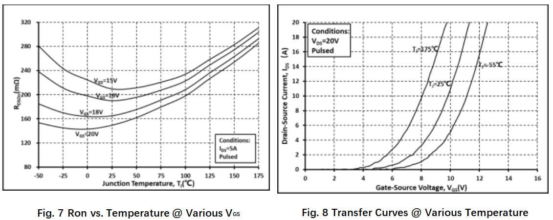
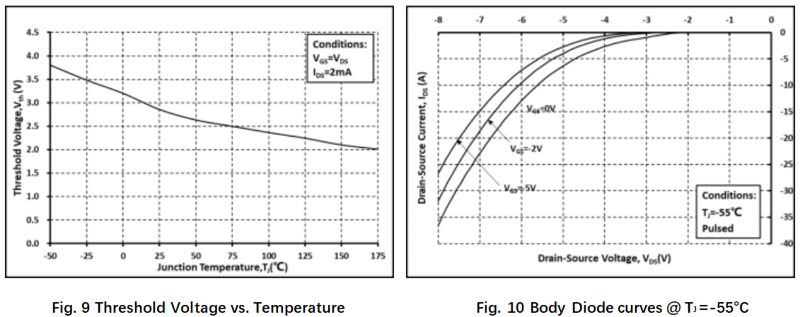
| VTH | Gate threshold voltage | 1.8 | 2.8 | 4.5 | V | VGS =VDS , ID =2mA | Fig. 8, 9 |
| 2.1 | VGS =VDS , ID =2mA @ TJ =175。C | ||||||
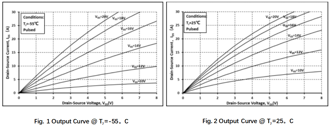
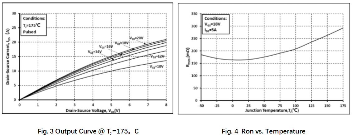
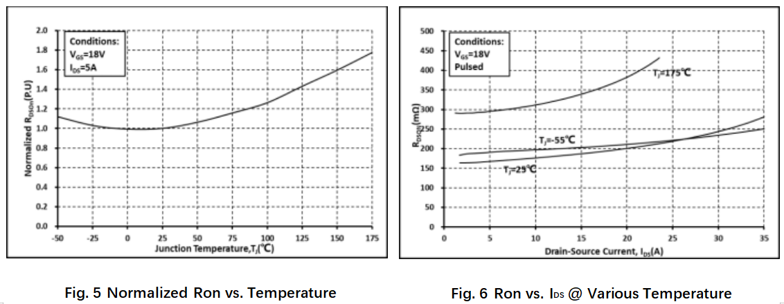
| RON | Static drain-source on - resistance | 160 | 208 | mΩ | VGS =18V, ID =5A @TJ =25。C | Fig. 4, 5, 6, 7 | |
| 285 | mΩ | VGS =18V, ID =5A @TJ =175。C | |||||
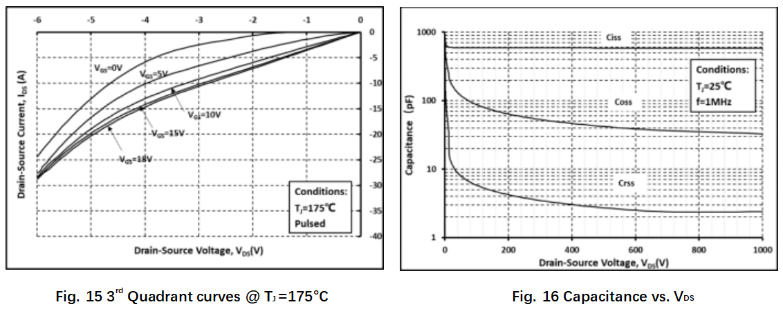
| Ciss | Input capacitance | 575 | pF | VDS=800V, VGS =0V, f=1MHz, VAC=25mV | Fig. 16 | ||
| Coss | Output capacitance | 34 | pF | ||||
| Crss | Reverse transfer capacitance | 2.3 | pF | ||||
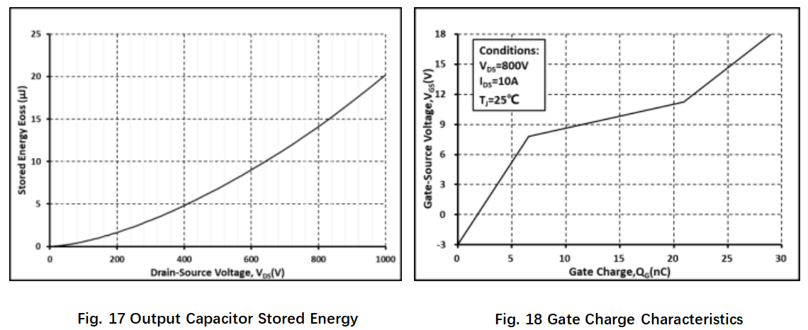
| Eoss | Coss stored energy | 14 | μJ | Fig. 17 | |||
| Qg | Total gate charge | 29 | nC | VDS =800V, ID =10A, VGS =-3 to 18V | Fig. 18 | ||
| Qgs | Gate-source charge | 6.6 | nC | ||||
| Qgd | Gate-drain charge | 14.4 | nC | ||||
| Rg | Gate input resistance | 10 | Ω | f=1MHz | |||
| EON | Turn-on switching energy | 115 | μJ | VDS =800V, ID =10A, VGS =-3.5 to 18V, RG(ext) =3.3Ω, L=300μH TJ =25。C | Fig. 19, 20 | ||
| EOFF | Turn-off switching energy | 22 | μJ | ||||
| td(on) | Turn-on delay time | 2.5 | ns | ||||
| tr | Rise time | 9.5 | |||||
| td(off) | Turn-off delay time | 7.3 | |||||
| tf | Fall time | 11.0 | |||||
| EON | Turn-on switching energy | 194 | μJ | VDS =800V, ID =10A, VGS =-3.5 to 18V, RG(ext) =3.3Ω, L=300μH TJ =175。C | Fig. 22 | ||
| EOFF | Turn-off switching energy | 19 | μJ | ||||
Reverse Diode Characteristics(TC =25。C unless otherwise specified)
| Symbol | Parameter | Value | Unit | Test Conditions | Note | ||
| Min. | Typ. | Max. | |||||
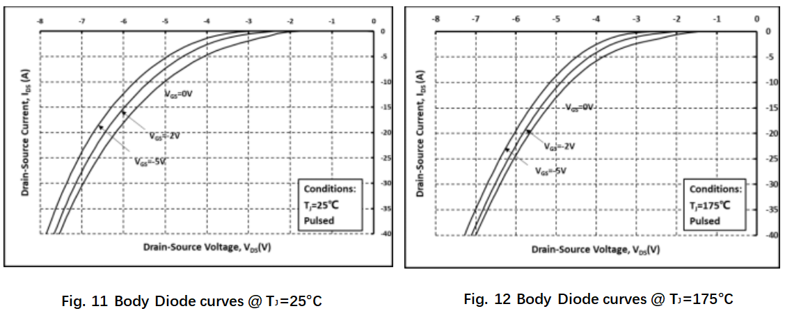
| VSD | Diode forward voltage | 4.0 | V | ISD =5A, VGS =0V | Fig. 10, 11, 12 | ||
| 3.7 | V | ISD =5A, VGS =0V, TJ =175。C | |||||
| trr | Reverse recovery time | 26 | ns | VGS =-3.5V/+18V, ISD =10A, VR =800V, RG(ext) =15Ω L=300μH di/dt=3000A/μs | |||
| Qrr | Reverse recovery charge | 92 | nC | ||||
| IRRM | Peak reverse recovery current | 10.6 | A | ||||
Typical Performance (curves)
